Studies of Dynamic Reverse Pulsing and Bipolar Reactive Sputtering of Silicon Oxide Films with No Detectable Inclusion of Anode Material
Posted October 13, 2020 by Philipp Dürrenfeld
The state-of-the-art Customer Solutions Lab was established to perform research, development, and customer product demonstrations for plasma/vacuum-based equipment and thin-film deposition/ characterization training – all aimed at driving the thin film industry forward and better serving the needs of our global customers. The Lab has an in-line coater and custom drum coater, both aimed at industry research and development. Additionally, the Lab hosts onsite metrology for electrical and optical properties as well as temperature measurement.
In our recent blog post, we demonstrated how silicon dioxide thin films can be sputtered with a reliably high quality and rate in an inline coating machine at our Customer Solutions Lab in Karlstein, Germany. Comparisons were made for films sputtered at a high argon flow, and thus higher-pressure, during deposition and a low argon flow and thus a lower deposition pressure. From the results, we estimated that the optimum conditions in terms of refractive index and stoichiometric composition of the SiOx films might lie in an intermediate pressure regime. We also saw a lower deposition temperature at an equal rate when we compared Dynamic Reversed PulsingTM (DRP) deposited films with those sputtered in a more conventional bipolar dual magnetron sputtering (DMS) configuration.
As a recap, DRP and DMS are two deposition configurations in a sputtering chamber equipped with two magnetron targets. DRP utilizes two synchronized power supplies and pulses the voltage for most of the time to the magnetrons with an additional floating anode as the counter-pole. The polarity is switched for a short time during each cycle – we use a 5% setting – to be reversed and the floating anode acts as the cathode. This is to keep the anode from being coated with an insulating film. In DMS, the power supply switches polarity in a 50/50-time share between both magnetrons, i.e. each target is acting as an anode for half of the time.
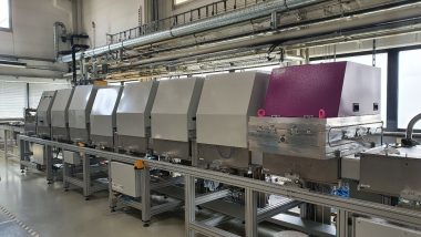
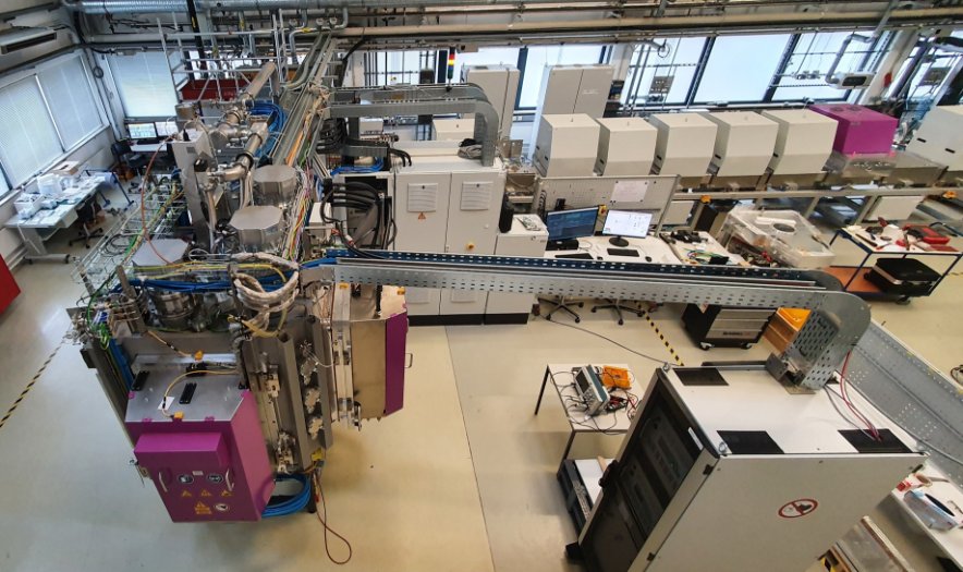
Figure 1: In-line coating machine at the AELab in Karlstein, Germany showing eight compartments. The sample carrier is inserted in the far left. Silicon oxide is dynamically deposited in the right compartment (purple hood) by moving the sample carrier beneath the rotatable magnetrons.
A picture of the in-line coating tool used for the depositions at intermediate pressure conditions (compared to the last settings) is shown in Figure 1. The two rotatable silicon targets are in the right compartment. Before starting each deposition, the argon flow of 30 or 35 sccm as well as the voltage from the power supply are fixed. The oxygen flow is then adjusted to yield the desired power in the transition mode. The substrate carrier is set to swing back and forth underneath the magnetrons at a fixed speed of 50 mm/s in order to capture the dynamic deposition rate. The number of swings is adjusted such that the resulting SiOx films all have a comparable thickness, irrespective of power and deposition rate.
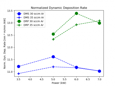
Figure 2: Normalized dynamic deposition rate of silicon oxide for DMS (blue) and DRP (green) at various sputtering powers.
The film thicknesses were measured by ellipsometry; from there, we calculated the dynamic deposition rate, i.e. the film thickness multiplied by the carrier moving speed, divided by the number of swings. To better visualize the differences in deposition rates, we show the dynamic deposition rate normalized to the total sputtering power (see in Figure 2). Note that for DRP the “total power” means the sum of the power at each power supply, i.e. at 7 kW, both Ascent DMS AP15s operate at 3.5 kW, compared to one Ascent DMS AP15 at 7 kW, in the case of DMS. At all points, DRP offers a significantly higher deposition speed compared to DMS, and the lead even increases for higher powers.
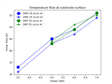
Figure 3: Total temperature difference during the deposition of silicon dioxide films by DMS (blue) and DRP (green)
A second important benchmark for comparing DRP and DMS is the heat load at the substrate. To measure this, we attached thermocouples to the top and bottom of a dummy glass wafer. A battery-powered datalogger (ECD Supermole) was inserted together with the sample into the vacuum chamber and continuously recorded the temperatures. Due to the dynamic deposition setting here, the temperature periodically increases with each swing, followed by a short cool-down time. As a temperature difference, we look at the maximum temperature over all swings and compare it to the temperature just before the deposition. DMS and DRP are compared in Figure 3, showing an increasing temperature rise for higher powers; yet no significant difference between DMS and DRP can be seen. However, knowing that the deposition rate in DRP is higher, we can state that DRP can deliver a faster deposition rate with the same heat load.
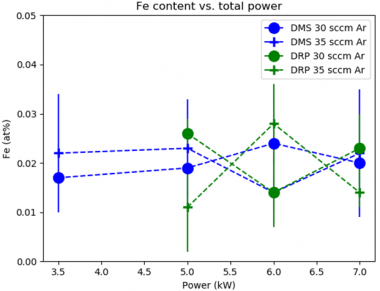
Figure 4: EPMA-detected iron content in the samples deposited with DMS (blue) and DRP (green). The content for all samples is near the detection limit and is not increased for DRP depositions.
The obvious difference between both deposition methods is the active inclusion of the additional anode in DRP sputtering. As this is connected to the power supplies, it takes part in the circuitry and acts – for a small adjustable amount of time – as a cathode. One might therefore ask whether any material from the anode is sputtered away and ends up in the deposited film, which would be undesirable. To test this, electron probe microanalysis (EPMA) was run on the deposited films with a dedicated investigation towards the iron content in the film. Iron was chosen because the anode is made of stainless steel. The resulting analysis data is shown in Figure 4, where it can be seen that the iron content stays constant and is always in the range of 0.02%. This value is near the detection limit, and within the measurement uncertainty, DMS and DRP deposited films have the same trace content. Thus, we could prove that no anode material is inadvertently incorporated in the deposited films for DRP.
The presented data confirms earlier results that reactive sputtering processes can benefit from the DRP configuration in such a way that the films are deposited at a higher rate with the same heat load on the substrate or conversely the heat load can be reduced while maintaining the same deposition rate. Having no additional anode material in the film when running DRP depositions proves that this configuration also means no compromise in the film quality when migrating from DMS.

Philipp Dürrenfeld
Related Posts
Blog
.jpg?resizemode=force&maxsidesize=884)