Dynamic Reverse Pulsing Enables High Deposition Rate at Lower Total Cost of Ownership for Reactive Sputtering on Heat-Sensitive Substrates
Posted April 07, 2020 by Philipp Dürrenfeld
You might not be consciously aware of it, but there’s a good chance one of the reasons you chose the smartphone you have is that it felt good in your hands. A lot of time, thought and research went into making it feel “just right” to you.
It’s not easy to achieve the desired properties in consumer devices or the expanding universe of applications. Thin film coating professionals face numerous challenges in standard and bipolar dual magnetron sputtering (DMS; see Figure 1). These include reducing and controlling process temperature for heat-sensitive substrates; power level limitations due to heat, material and current; and anodes that “disappear” in high deposition rate configurations. Of course, there’s always the objective to reduce costs wherever possible.
Dynamic Reverse Pulsing (see Figure 1) eliminates those pain points by lowering the heat and increasing the deposition rate, requiring fewer chambers, and increasing throughput of existing coaters without the expensive addition of cathodes, lids and zones. Advanced Energy introduced DRP, a power configuration technology marked by enabling a higher deposition rate, lower substrate heating and higher power output on magnetrons, in 2015.
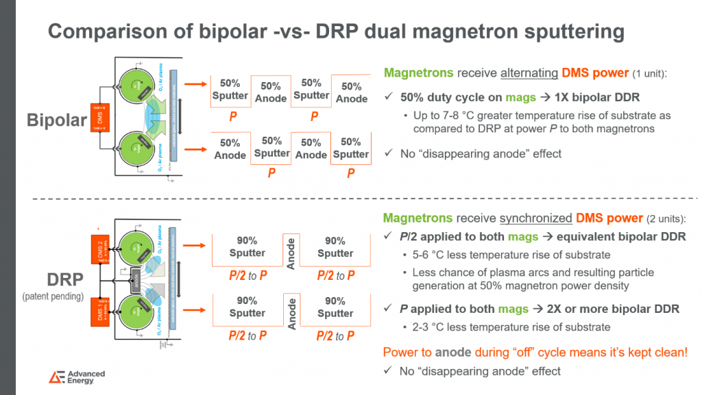
Figure 1. Bipolar versus DRP (patent pending) dual magnetron sputtering configurations
DRP’s unique capabilities transform the paradigm for reactive sputtering, enabling new processes that achieve desired deposition rate and material properties uniformity. DRP also presents an unconventional power system configuration offering new economic benefits to customers. Those benefits are being demonstrated both in customer installations and in our AE’s Customer Solutions Lab.
Additionally, in high-volume consumer device coating, using DRP-configured coaters can offer savings in capital investment (CapEx) by reducing the overall number of coaters needed for high volume production.
Data shared by many of our customers within the last couple years shows one of three results:
- Either the deposition rate can be more than doubled using the patented plasma power configuration in a dual magnetron arrangement;
- The substrate temperature can be decreased by several oC, which is very important for heat sensitive substrates like polymers; or
- A combination of the two outcomes!
The bottom line is lower substrate heating during deposition at a higher rate of deposition. Up to 2.4X has been measured, as compared to bipolar dual magnetron sputtering, at several of our customer installation sites.
What was not presented is DRP’s impact on the deposited coating’s material properties. So, BIG questions remained unanswered:
- Do the DRP benefits of increased deposition rate and/or reduced temperature adversely or positively affect the resulting material’s quality?
- Or, does the thin film material properties remain unaffected?
Honestly, we just didn’t know…until now!
Answers to critical questions
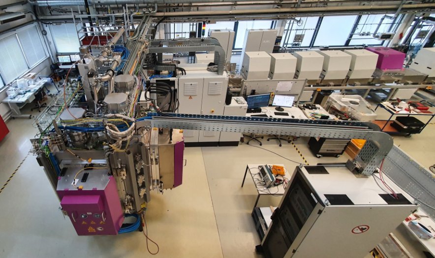
We recently opened our Customer Solutions Lab, located near Frankfurt, Germany, established to perform research, development, and customer product demonstrations for plasma/vacuum-based equipment and thin-film deposition/ characterization training (see Figure 2). Over the past several months, the lab team has completed its first set of experiments, where both a standard bipolar configuration and a DRP dual magnetron sputtering configuration were used to deposit silicon oxides, SiOX, where X is the thin film’s elemental stoichiometry. When X = 2, stoichiometric silicon dioxide (SiO2) is formed. SiO2 thin films are important for various applications, such as providing passivation or electrical insulation in numerous applications – e.g. flat panel displays and thin-film transistors, for decorative coatings for mobile electronics on various materials including heat sensitive plastics, for solar/photovoltaic and more!
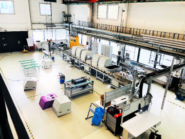
Figure 2. The AE plasma laboratory from its mezzanine, showing rotatable dual magnetron sputtering cathodes with silicon (Si) targets removed from its adjacent SOLAYER H500 GEN 2.0 multi-chamber inline coater.
Material properties measured at the Customer Solutions Lab and/or at Fraunhofer IST in Braunschweig, Germany include:
- SiOX elemental stoichiometry X measured by electron probe micro-analysis (EPMA);
- Elemental depth analysis measured by secondary ion mass spectroscopy (SIMS);
- Refractive index n, extinction coefficient k and thickness t with thickness uniformity measured by ellipsometry (thicknesses verified via physical surface profiler and SIMS);
- Thin film surface roughness deposited on various substrates measured by atomic force microscopy (AFM);
- Optical transmission and absorption properties, and more.
All DRP-deposited SiOX/2 material properties are equivalent to bipolar sputtered SiOX/2 material properties. As an example, please see the coating’s refractive index n (measured via ellipsometry at wavelength l = 550 nm) in Figure 3. When n = 1.458, the deposited material’s refractive index is equal to thermally grown SiO2 on silicon in a semiconductor grade furnace at 1,200 oC. This was achieved for the DRP-deposited SiO2 coatings only.
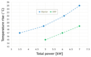
Figure 3. Temperature rise of the glass substrate as measured in situ by an ECD SuperM.O.L.E. thermal profiler at comparable deposition rates. The deposition rate increases with the total power but is virtually the same at the same total power between both configurations. However, each DRP cathode only observes approximately 50% of the power density as compared to the bipolar configuration, which also leads to less plasma arcs and resulting particle generation. The temperature rise is 5-6 oC less for DRP as compared to standard bipolar configurations.
What’s next at AE’s Customer Solutions Lab?
The Customer Solutions Lab team plans to continue investigating bipolar configurations versus DRP in SiOX experiments. Many more important application materials will be investigated in the years to come. This includes depositing DRP SiOX/2 thin films onto actual heat-sensitive substrates and comparing to bipolar DMS results.
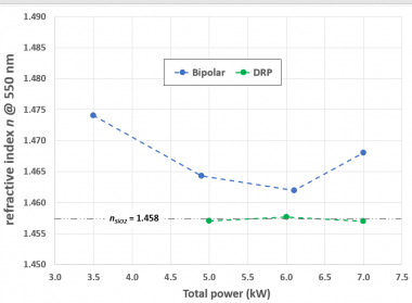
Figure 4. Refractive index n measured via ellipsometry (at a wavelength of ƛ = 550 nm) as a function of DMS bipolar power generator’s total power P applied to the plasma. Thermally grown SiO2 on Si substrates in a semiconductor grade furnace has an n = 1.458. Therefore, the DRP deposited SiO2 coatings are virtually identical to thermally grown SiO2, where in this case the standard bipolar deposited SiOX coatings are not. In this study, all other measured material properties are equivalent or better for DRP SiOX films.

Philipp Dürrenfeld
Related Posts
Blog
.jpg?resizemode=force&maxsidesize=884)