The Future of Semiconductor Manufacturing: Reflecting on the 2022 SEMI Industry Strategy Symposium
Veröffentlicht April 19, 2022 von Edwin Mok
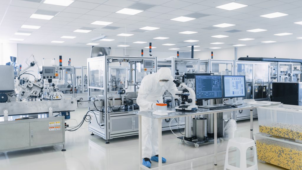
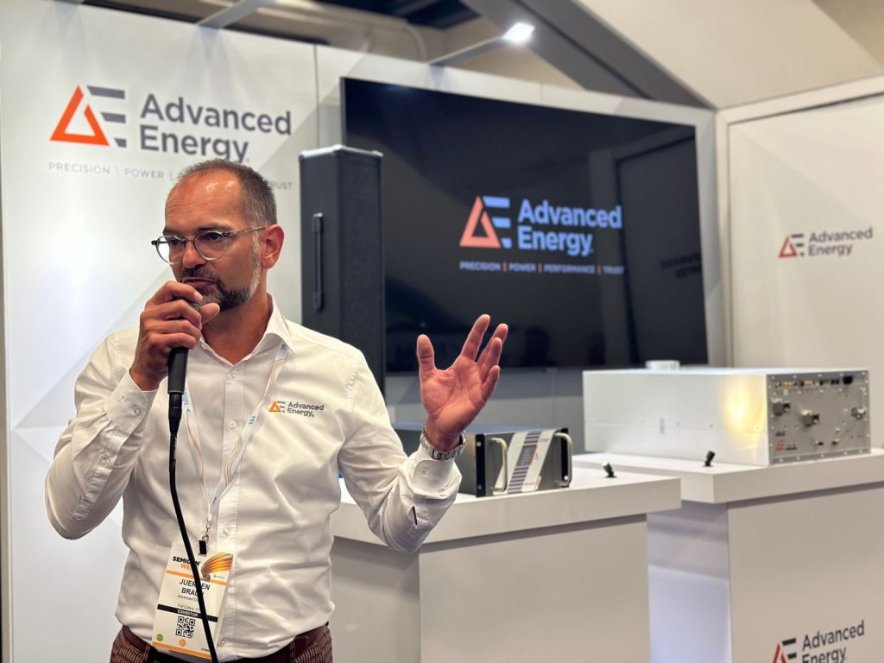
As a market leader in precision power conversion, measurement and control solutions for semiconductor manufacturing, Advanced Energy has long been a participant at SEMI’s Industry Strategy Symposium (ISS), the premier event to share the semiconductor industry’s outlook. Despite this year’s off-cycle event in April (compared to the typical mid-January), ISS saw record attendance.
The Importance of the Semiconductor Industry
A desire to better understand macro uncertainties and a strong Wafer Fab Equipment (WFE) market likely incentivized ISS attendance. A quick sweep of media headlines over the past two years highlights the growing significance of semiconductors to more and more industries. Entering 2022, there are increased uncertainties of the broader economy from supply chain constraints to inflation and rising interest rates and - more than ever - the entire semiconductor supply chain is playing a more important role as a “behind the scenes” driver of the economy. More government officials from both the federal and state level attended this year’s ISS, highlighting the growing importance of semiconductors to national security, the U.S. government’s focus on strengthening the semi supply chain, as well as new opportunities for governments to invest in supporting the semi equipment and materials companies.
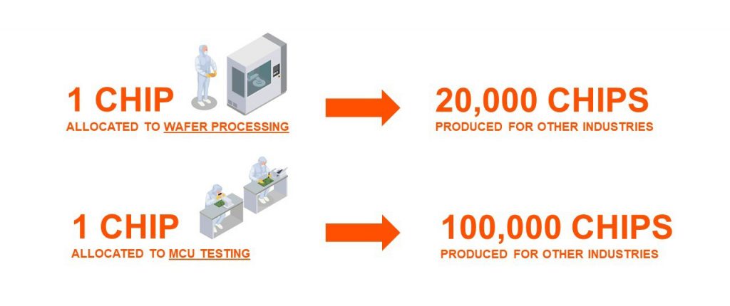
While the 2022 forecasts and the long-term outlook are equally optimistic, with some predicting that the semiconductor industry will reach $1 trillion in sales by 2030 followed closely by the semi equipment and materials industry, most agree that the supply chain remains the biggest risk. Several analysts believe that a downturn will likely occur before we reach this milestone given the cyclical nature of the industry but the timing of such a downturn is a subject of contention. The resolution of supply constraints will be critical to growth in 2022 and 2023. To improve supply constraints, chips must be allocated to the semi equipment industry to enable the creation of more chips. According to SEMI, each chip allocated to a wafer processing tool will produce at least 20,000 additional chips per year, and each FPGA allocated to a microcontroller (MCU) tester will test nearly 100,000 additional MCUs per year. One chip used in the semiconductor equipment industry produces many more chips for automotive, consumer electronics, data centers and other industries.
Semiconductor Process Technology Innovation
Resolving supply constraints is also critical to the pace of innovation beyond the semiconductor industry. At ISS, chipmakers highlighted the dependence of disruptive technologies such as Artificial Intelligence (AI) and Machine Learning (ML) on the semiconductor industry. The advancement in the leading-edge wafer processing and in advanced packaging processes have been critical to enable AI and ML applications. The exponential growth of AI computation usage is faster than Moore’s Law, powered by the substantial improvements in processor performance, as well as innovation in the wafer processing and equipment industry.
Three major technology trends are poised to drive advancements in leading-edge logic over the next several years:
1. Gate All Around at 2nm/1nm and CFET for <1nm
Gate-All-Around (GAA) is the most immediate technology inflection for the industry and allows the industry to continue to follow Moore’s Law. As advanced logic moves to 2nm node, GAA will be adopted by all three leading-edge companies. Since 2nm is already in development, GAA is currently the key battleground for leading equipment OEMs. The architectural change from FinFET to GAA will require many new process steps, which will ultimately drive increased demand for advanced etch, deposition, epi and PEALD process equipment. At ISS, Tokyo Electron detailed the process complexity of creating a GAA device and ASM discussed its new PEALD processes to create nanotube gates. In addition, LAM Research recently launched new etch products designed for GAA.
At Advanced Energy, we have been working closely with our OEM customers to develop next-generation process power solutions that will enable many of those new processing steps necessary to create future generation of devices, from Nanosheet GAA and Forksheet GAA to CFET and beyond.
2. Backside power
Chipmakers are targeting to change the back-end-of-line (BEOL) interconnect to substantially drive improved power efficiency and transistor density, critical to enable continued scaling down to sub-2nm and beyond nodes. Historically, BEOL is created after the transistors are formed on the wafer but new backside power architecture intends to move a number of metal layers to the “back” by sandwiching the transistors between front and back side metal layers. This is done by creating two individual wafers and attaching them together. The shift to backside power will require new etch and deposition processes to create the interlayers, with new process steps and films likely to be required. To enable this change, new processing power solutions and potentially new breakthrough power deliver solutions will be needed. Advanced Energy has been the market leader in process power solutions and will continue its leadership in enabling many next-generation etch, depositions, implant, inspection and other processing tools.
3. Chiplet or die stacking in 3D packaging
2.5D and 3D packaging have already been widely used across many semiconductor devices but this is just the beginning. Known as chiplets, dies or tiles of different function are integrated together using advanced packaging techniques to create more powerful chips that are also more cost efficient. Much has been written about the variety of 2.5D/3D package structures but at this year’s ISS, there is growing evidence of the increased innovations that are being developed to create these complex packages. From AMD’s transition to a 3D chiplet that comes with over 200X increase in interconnect density to Intel’s next-gen Foveros Direct technology with 40x interconnect bump density, there is less separation between wafer processing and packaging in chiplet architecture. Historically, the industry mostly used tools built for wafer processing or legacy packaging equipment to create the 2.5D packaging architectures. However, new technologies and equipment are being developed specifically to create 3D packages. Naturally, the new equipment will come with new and likely more complex power requirements and Advanced Energy is ready to meet these challenges.
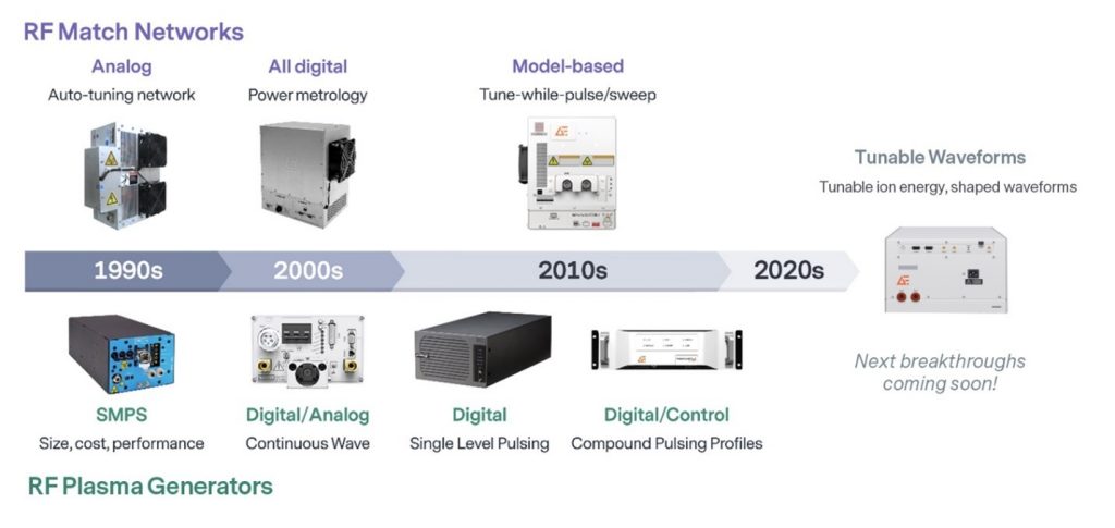
Over the past 40 years, Advanced Energy has been at the forefront of developing next-generation power solutions to drive advanced nodes. AE continues to innovate the future of power in semiconductor manufacturing processes. The heart of critical etch and deposition processes will continue to be plasma-driven, led by a new generation of plasma power solutions such as Advanced Energy’s eVoS™, our asymmetric bias waveform generator, and Navigator II FCi, our high speed solid state match.
Workforce Development and Diversity & Inclusion
It’s an exciting time for the industry, with advances in semi manufacturing processes translating into innovations in intelligent, revolutionary technologies that touch and improve all aspects of life. But for the semiconductor industry to move forward, workforce development and diversity and inclusion must be at the forefront. It was encouraging to hear the efforts the semiconductor industry has put into nurturing a diverse, workforce-ready talents at ISS with presentations from industry thought leaders, leading companies, universities and students. It was also exciting to hear presentations from a diverse group of students and get a glimpse of the next-generation of industry leaders. One solution to address the under-representation of minority groups is to expand the talent pipeline and allow students from these groups to explore opportunities in STEM. For example, Advanced Energy’s STEM Diversity Scholarship Program aims to develop emerging talent and promote greater diversity in STEM. Not only does this help fill the industry pipeline with qualified talent, the program also cultivates new and different perspectives that help drive technological innovations that positively impact society.
Edwin Mok
Verwandte Beiträge

Blog
Model-Based Frequency Tuning Revolutionizes RF Power Delivery
Blog
SEMICON West 2023: AE Advances the Angstrom Era with Transformational New Technologies
Blog