Trends from SEMICON® Korea 2026
Veröffentlicht März 24, 2026 von Juergen Braun
SEMICON Korea 2026 took place from February 11 to 13 in Seoul, South Korea, and is a highly regarded tradeshow in the semiconductor industry. Advanced Energy was present at the show, highlighting products and capabilities that address some of the industry’s latest trends.
In South Korea, high volume memory production is shifting focus towards high-bandwidth memory (HBM) to meet increasing demand for artificial intelligence (AI) applications, data centers and semiconductors. Dynamic random-access memory (DRAM) architecture has moved from 2D planar structures to advanced 10 nm-class nodes (1a, 1b, 1x) and potentially 1d and 4F2 nodes to address faster, more efficient and high-density memory solutions.
With this in mind, there were three notable trends at SEMICON Korea where Advanced Energy is playing a key role in.
Three trends observed at SEMICON Korea
1. Yield as the Top Priority
Yield emerged as the defining theme of the trade show, with prominence across multiple booths, presentations and panel sessions.
As the industry moves towards the mass commercialization of HBM4 memory to more efficient and high-density DRAM and NAND technologies, manufacturers repeatedly emphasized the need for advanced metrology and inspection solutions that can detect defects in the deeply stacked and ultra fine structures of these devices.
This reflects a broader shift away from “scaling for performance,” which has been a mantra until now, and instead moves towards “scaling with defect free precision.”
2. Artificial Intelligence-Driven R&D and Process Optimization
Also in the forefront was a belief stressed by virtually every major chipmaker – that traditional research and development (R&D) models can no longer keep pace with shrinking geometries and higher complexity.
This was particularly well said in a presentation on AI based R&D acceleration, which demonstrated how AI is being used to reduce experiment cycles, optimize process variables, and enable the faster development of new materials and device structures.
3. Expanding Collaboration to Address Industry Challenges
Through programs such as the AI Summit (SEMI × KAIST) and technical symposia, industry leaders are coming together to align on technology roadmaps for next generation memory, advanced packaging, and smart manufacturing. In parallel, collaborative efforts are being established to regulatory challenges and supply chain resilience related to per- and polyfluoroalkyl substance (PFAS) chemicals. The event underscored South Korea’s growing importance as a central hub for semiconductor innovation in the AI era.
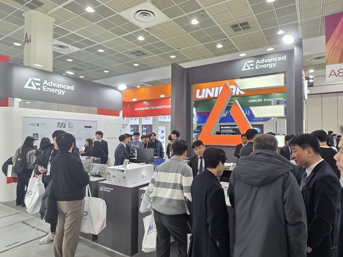
 Fig. 1 Advanced Energy showcased a range of precision power and measurement solutions for the semiconductor industry at its booth, #A654 this year
In South Korea, high volume memory production is shifting focus towards high-bandwidth memory (HBM) to meet increasing demand for artificial intelligence (AI) applications, data centers and semiconductors. Dynamic random-access memory (DRAM) architecture has moved from 2D planar structures to advanced 10 nm-class nodes (1a, 1b, 1x) and potentially 1d and 4F2 nodes to address faster, more efficient and high-density memory solutions.
With this in mind, there were three notable trends at SEMICON Korea where Advanced Energy is playing a key role in.
Three trends observed at SEMICON Korea
1. Yield as the Top Priority
Yield emerged as the defining theme of the trade show, with prominence across multiple booths, presentations and panel sessions.
As the industry moves towards the mass commercialization of HBM4 memory to more efficient and high-density DRAM and NAND technologies, manufacturers repeatedly emphasized the need for advanced metrology and inspection solutions that can detect defects in the deeply stacked and ultra fine structures of these devices.
This reflects a broader shift away from “scaling for performance,” which has been a mantra until now, and instead moves towards “scaling with defect free precision.”
2. Artificial Intelligence-Driven R&D and Process Optimization
Also in the forefront was a belief stressed by virtually every major chipmaker – that traditional research and development (R&D) models can no longer keep pace with shrinking geometries and higher complexity.
This was particularly well said in a presentation on AI based R&D acceleration, which demonstrated how AI is being used to reduce experiment cycles, optimize process variables, and enable the faster development of new materials and device structures.
3. Expanding Collaboration to Address Industry Challenges
Through programs such as the AI Summit (SEMI × KAIST) and technical symposia, industry leaders are coming together to align on technology roadmaps for next generation memory, advanced packaging, and smart manufacturing. In parallel, collaborative efforts are being established to regulatory challenges and supply chain resilience related to per- and polyfluoroalkyl substance (PFAS) chemicals. The event underscored South Korea’s growing importance as a central hub for semiconductor innovation in the AI era.
Fig. 1 Advanced Energy showcased a range of precision power and measurement solutions for the semiconductor industry at its booth, #A654 this year
How Advanced Energy fits into the ecosystem
Advanced Energy (AE) is a leader in enabling both the precise, real-time understanding of the conditions within the chamber, and delivering power with the precise control and near instant matching that allows even the most complex recipes to be undertaken.
The shift to Angstrom-Era processes takes this a step further and it’s no surprise that there was a significant interest at the show for a range of products including AE’s eVerest® RF generator, its matching network, NavX™, and the eVoS® bias platform. These new platforms offer greater process control helping customers improve yield on their tools. In addition, PowerInsight by Advanced Energy® is a comprehensive data acquisition and analysis tool that leverages high-resolution process data to enable faster characterization, development and troubleshooting.
Additionally, AE showcased a wide array of sensing products including the OR4100T, OR401M, Luxtron® M1200 and Tegam® 5540A, which offer an exceptionally accurate method for monitoring process conditions in the chamber. Also on display was AE’s Omni™ RF diagnostic cart, which enables RF calibration and diagnostics for the maintenance of semiconductor fabrication systems.
AE’s Thyro-XD™ generated significant interest thanks to its class-leading resistance measurement accuracy, which enables users to precisely control chuck-heater temperature indirectly through the linear change in resistance with temperature.
Finally, AE demoed a brand-new power controller technology with variable amplitude sinusoidal output that provides virtually zero harmonic distortion.
At SEMICON Korea, Advanced Energy demonstrated that leadership in precision power, measurement and control solutions is helping the industry move confidently into the next phase of semiconductor growth. As fabs accelerate advanced nodes and AI driven manufacturing, AE is focused on delivering the innovations that turn scale, yield and reliability into real production advantage.
There will be greater leaps forward in semiconductor manufacturing this year as 2 nm is commercialized and even smaller process nodes are developed. Attendance at this show has demonstrated that South Korea is central to the world’s ever-growing semiconductor ramp. It has highlighted that Advanced Energy continues to be aligned with key stakeholders in this region as it seeks to drive cutting-edge innovation and meet the increasing demand.
For more information about Advanced Energy’s expertise in the semiconductor industry, visit: Semiconductor | Precision Power Delivery and Thermal Control Solutions | Advanced Energy | Advanced Energy.

Juergen Braun
Advanced Energy
Juergen Braun joined Advanced Energy in July 2007 and now serves as senior vice president of plasma power products. In his current role, Braun leads the plasma power and service business. Prior to his current role, he held several leadership positions within the company including vice president and general manager of the thin film group, general manager of the photonics group, and managing director of Advanced Energy’s EMEA sales office. Braun brings over 20 years of experience in semiconductor manufacturing with a successful record of implementing strategic business plans, leading cross-functional international teams, as well as delivering revenue and market share growth. Braun holds a Diploma in chemistry from the University of Ulm, Baden-Württemberg, Germany, where he also completed his Ph.D. thesis on CVD growth of silicon and germanium on Si.
Mehr Beiträge von Juergen Braun
durchsuchen
Kategorien A-Z
Tragen Sie sich in unsere Mailingliste ein
Abonnieren
Neueste Beiträge
View on X