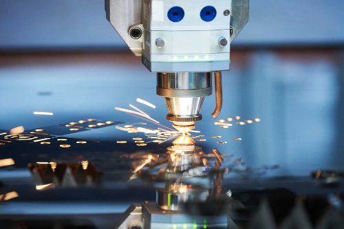
剥离
通过精确控制功率实现完美晶圆剥离
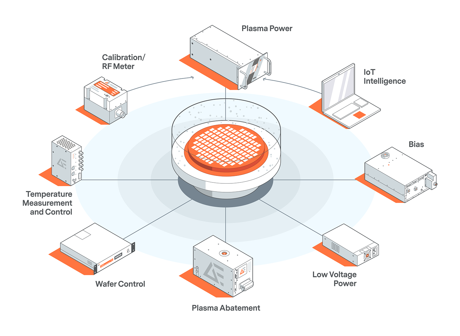
去除残留的光刻胶,对于确保高质量产品至关重要。Advanced Energy 的等离子电源输送系统、交流/直流和直流/直流前端电源以及机架系统产品组合能够以可控、高效的方式提供去除光刻胶所需的精确功率。我们的产品设计始终致力于优化效率和功率密度,在降低总拥有成本的同时确保可靠性和长时间正常运行。AE 的各种行业标准板载电源模块得到原始设备制造商和系统集成商的广泛应用,可提供半导体制造商所需的灵活性和可扩展性,满足剥离工艺的要求。
特色产品


相关博客
All BlogsModel-Based Frequency Tuning Revolutionizes RF Power Delivery

Blog
Model-Based Frequency Tuning Revolutionizes RF Power Delivery
The Next Leap: Powering Plasma for the Angstrom Era
Key Takeaways:
- Semiconductor manufacturing is advancing rapidly.
- Innovations in process equipment and power delivery technologies enable the creation of devices with atomic-scale dimensions.
- The industry is moving into the Angstrom Era, increasing the complexity of manufacturing processes.
- Exceptional agility and control in plasma power delivery systems are required.
- Advanced Energy is at the forefront of these innovations.
- They provide sophisticated RF plasma power solutions supporting advanced-node device development.
- New technologies offer precise control, high-speed responsiveness, and improved energy management.
- These advancements are essential for the next generation of semiconductor devices.
Semiconductor manufacturing pushes the boundaries of process innovation to the nearly impossible. Reaching a new device node is the culmination of vision, technology and partnership. These leaps forward are enabled by both possibility and capability. Often, the difference between the impossible and the next node comes down to process equipment innovations that open wholly new windows of performance and functionality.
Complexity is spiraling upwards. Higher feature densities are leading to 3D structures and novel transistor architectures with dimensions on the atomic scale, measured in angstroms (10-10 meters). Altogether, this demands unprecedented process control. Advanced-node devices drive ambitions for innovative process equipment — including extraordinary power-delivery technologies — to expand the limits of the possible.
Radio frequency (RF) plasma power delivery systems have evolved to become highly sophisticated power control engines with ultrafast responsiveness — as different from earlier RF generators as a thoroughbred horse is from a donkey. High-speed, precise power delivery enables radical changes and industry inflections from chip-scale packaging through advanced front-end technologies including gate-all-around (GAA) transistors, backside power delivery (BPD) and the path to 3D DRAM.
As the semiconductor industry ventures into the Angstrom Era, plasma processes used to create these extraordinary devices require exceptional agility, complex pulsing sequences with near-instant tuning speeds, recipe-customizable control capabilities and, increasingly, direct control of the plasma ion energy that creates the devices.
Advanced Energy has been making impossible plasma processes possible for over 40 years. AE is once again leaping forward in plasma control by introducing transformational power delivery technologies to address the challenges of the Angstrom Era.
A History of Transformational Power-Delivery Solutions
The semiconductor industry has relied on AE’s plasma power innovations to jump from micron to submicron to nanometers and now to angstrom-dimension devices
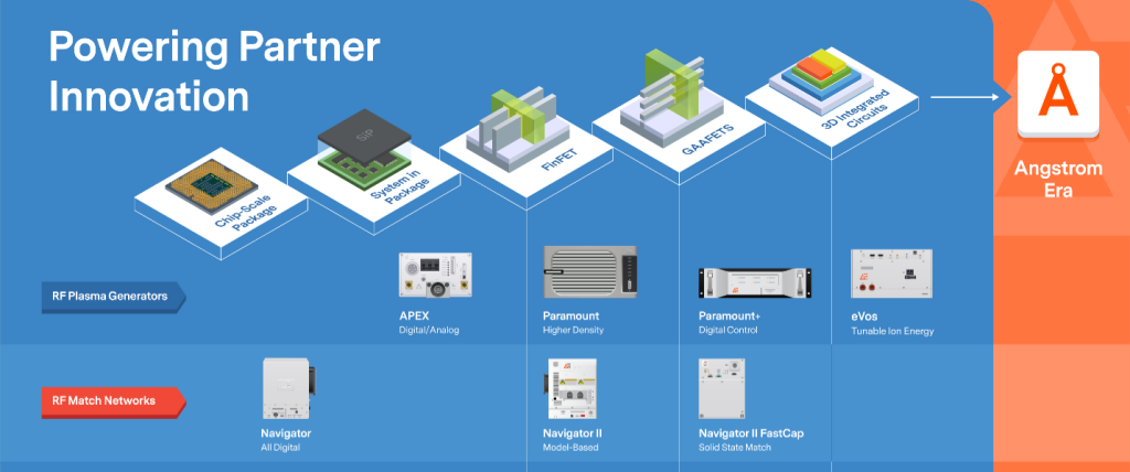
These innovations have been instrumental in supporting leading-edge plasma processes starting from the chip-scale era when all-digital Navigator® technology provided three to five times the match speed and unsurpassed RF metrology compared to competing products. The sophistication of AE power delivery and match technology grew across the next chip design nodes, providing increasing precision, power density, performance features such as pulsing, as well as faster response to abruptly changing plasma conditions. Advanced Energy’s eVoS™ platform is an example of the kind of revolutionary power technology capabilities that change what’s possible in plasma processing with its direct ion energy control. And there’s more to come.
Leaping into the Angstrom Era
Process recipes are more complex than ever, with multiple steps as short as one second transitioning through very different plasma conditions — often without turning off power to the plasma. Nimble, reproducible, repeatable RF plasma power delivery is vital to manage the extreme swings in plasma impedance caused by frequent, abrupt and profound changes in gas flow, chemistry, pressure and power. In the most advanced deposition and etch processes, critical aspects include precise control of target-species energy and repeatability from wafer to wafer in highly non-linear plasma environments.
AE addresses these challenges with a leap ahead in plasma power control, providing the agility, stability and speed required to drive Angstrom-Era semiconductor applications. This new, forward-looking technology provides critical performance:
- Speed of control within pulse profiles
- Power overhead for reliable ignition
- Waveform customization and control
- Ion energy management via direct plasma sheath voltage control
- Interconnected, coordinated operation of all power delivery components on complex plasma wafer processing equipment
- IoT ecosystem: High-resolution, high-bandwidth data access and sophisticated analytics
Transcending the Impossible: Powering the Future
From its inception, the semiconductor industry has constantly pushed the physical limits of device dimensions, densities and speed. Continuing the march from nanometer to angstrom device dimensions will be a truly remarkable milestone. Evolutionary and revolutionary advances in process power will provide the drumbeat bringing this vision to fruition. Those at the forefront of plasma power delivery technology will be the primary enablers as the industry draws closer to once-impossible dimensions.
Preview AE’s new, transformational power delivery technology, which will be available this summer.

SEMICON West 2022: SEMI Goes Big; Chips Get Small
What was new this year at SEMICON® West? This July, semiconductor professionals gathered virtually and in person at the Moscone Convention Center to make connections, exchange ideas, and discover what’s on the horizon for the industry. The ability to have face-to-face conversations, shake hands, interact with live demos, and see booths in three dimensions was a refreshing return to tradition. It was clear that everyone was glad to be back, and for me, the temperate climate of San Francisco was a reprieve from the heat of Colorado.
In past years, we mostly saw industry veterans at the show, but this year, our team at the booth spoke with several interns and new employees in purchasing, test engineering, and design engineering who were eager to learn. It was especially interesting to see the high level of interest in new opportunities in the semiconductor industry at the Workforce Development Pavilion, which provided one-on-one mentoring from semiconductor professionals to grow the talent pipeline.
Opportunities, Challenges, and Milestones: The Future of the Industry
One keynote at the SEMI® Market Symposium predicted that, driven by AI, the industry will surpass $1 trillion by 2030—but not without challenges. Current shortages are driving supply chain regionalization and vertical integration, while manufacturing regionalization offers the opportunity to implement basic improvements to sustainability, workforce talent, and supply base. Other topics of the symposium included the semiconductor technologies interacting with high-performance cloud computing, fab trends and forecasts, and global economic trends that will affect the future of the industry. Of course, shrinking feature sizes and new architectures are always hot topics as the industry sets its sights on Angstrom-level processing.
Additional forecasts from SEMI included:
- 14.7% rise in global sales of total semiconductor manufacturing equipment by OEMs to a record $117.5 billion in 2022, followed by an increase to $120.8 billion in 2023
- 15.4% expansion of the wafer fab equipment segment in 2022 to a new industry record of $101 billion, followed by a 3.2% increase to $104.3 billion in 2023
- Taiwan, China, and Korea remaining the top three equipment buyers in 2022
Building on recent years, sustainability was a big topic throughout the week. As President Biden unveiled new executive actions to combat climate change, key leaders from top OEMs and end users underscored rapid technological developments with sustainability in mind.
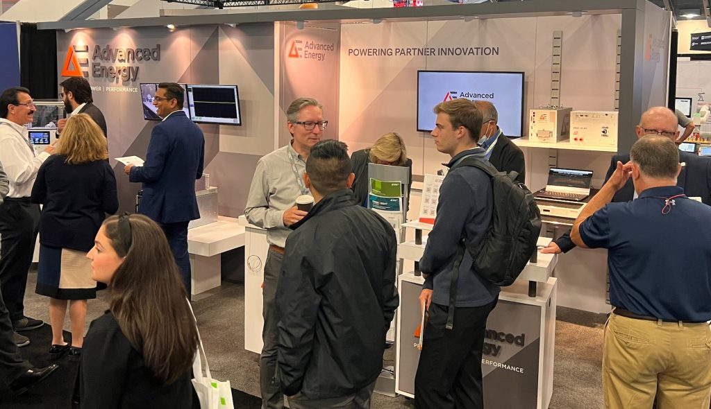
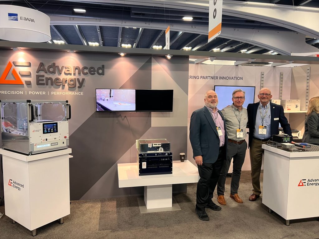
Powering Partner Innovation: Advanced Energy at SEMICON West
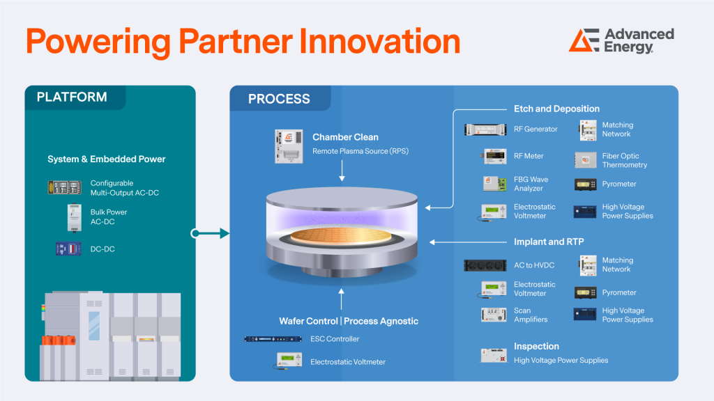
As the industry sets its sights on big financial growth, ever-smaller device geometries, and increased environmental stewardship, the Advanced Energy® team was excited to be back in person to share our pioneering approach to meeting today’s semiconductor manufacturing requirements, solving the toughest customer challenges, and enabling technological development as we head toward Angstrom-level processing.
With that in mind, we presented solutions for the critical etching, deposition, inspection, implantation, and annealing processes that propel the industry into the future, displaying an expanded range of power and measurement solutions that maximize productivity for a variety of platform and process requirements. This included remote plasma sources, pulsed power supplies, AC/DC power supplies, RF generators, matching networks, amplifiers, and high-accuracy temperature-sensing modules.
Product Highlights
Our Plasma Power Generators Group featured:
- The Ascent® SMS AP 10 kW pulsed-DC power supply, which delivers unprecedented plasma control in a compact solution for single-magnetron sputtering.
- PowerInsight by Advanced Energy™ monitoring and analytics platform, which brings actionable intelligence and insights to critical power-delivery systems, allowing owners to maximize performance, improve yield, and increase throughput.
Our industrial specialists featured:
- AE’s new Luxtron® M-1100, a single solution that enables manufacturers to monitor and control processes across extended temperature ranges.
- The software-driven Trek® 646 electrostatic chuck supply used in a variety of semiconductor processes to hold the wafer during processing.
These are just a few of the power delivery, sensing, and control solutions we presented at the show.

Blog
SEMICON West 2022: SEMI Goes Big; Chips Get Small
The High-Voltage Innovations Behind Moore’s Law
Anyone associated with the semiconductor industry – and many people who aren’t – will be familiar with Moore’s Law, the concept that the number of transistors (and, thus, the processing power) per unit of integrated circuit (IC) area doubles every two years. Putting it in perspective (as a notice in the Intel Visitor Center makes clear), if the principles of Moore’s Law had been applied to the airline industry the way they have to the semiconductor industry, then a commercial flight between New York and Paris that cost $900 in 1978 would now cost about a penny and take less than one second.
While debate continues about how long this principle can continue, it has served the industry well for almost sixty years and continues to be relevant as semiconductor manufacturers drive the capabilities of their chips to ever-new heights.
Behind the advanced functionalities and processing performance of the latest generations of semiconductors are sophisticated and truly transformative wafer fabrication processes. These processes are expected to deliver high yields with maximum productivity and minimum downtime, even as complexity, temperature and power demands rise. Many of wafer fabrication processes are enabled by precisely controlled, reliable high-voltage power systems, and without these critical sub-systems, the process equipment will not be able to meet the increasingly challenging requirements. And with the global semiconductor industry expected to reach $600 billion for the first time in 2022 - and many manufacturers announcing new fabs - the demand for high-voltage power systems is growing rapidly.
High-Voltage Power for Mission-Critical Systems
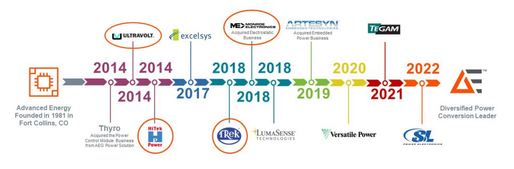
As a leader in engineering mission-critical high-voltage equipment for demanding applications, Advanced Energy has been addressing the power demands of the semiconductor sector for over forty years. In the last decade, the company has further accelerated the expansion of its high-voltage technology and IP portfolio (100 V to 300 kV) through the acquisitions of high-voltage power supply provider UltraVolt, high-voltage power conversion specialists HiTek Power, high-voltage power amplification and electrostatics specialist Trek, and the electrostatic instrumentation business of Monroe Electronics.
Advanced Energy’s growth results in a comprehensive portfolio for critical high voltage systems,enabling our customers’ transformative manufacturing technologies
The result is a comprehensive portfolio of solutions for many semiconductor fabrication power requirement, including ion implantation, deposition, etching, e-beam lithography, process metrology and inspection, as well as semiconductor testing. This portfolio combines over 1,500 standard products encompassing high-voltage power supplies, high-voltage amplifiers, power and control systems for electrostatic chucks and electron beam power solutions for a number of e-beam processes. Many of these products offer high levels of flexibility and modularity to allow engineers to precisely match the widest possible range of system specifications. In addition, engineering capabilities and proven technology support the building of custom high-voltage power supplies through close collaboration with design and application experts.
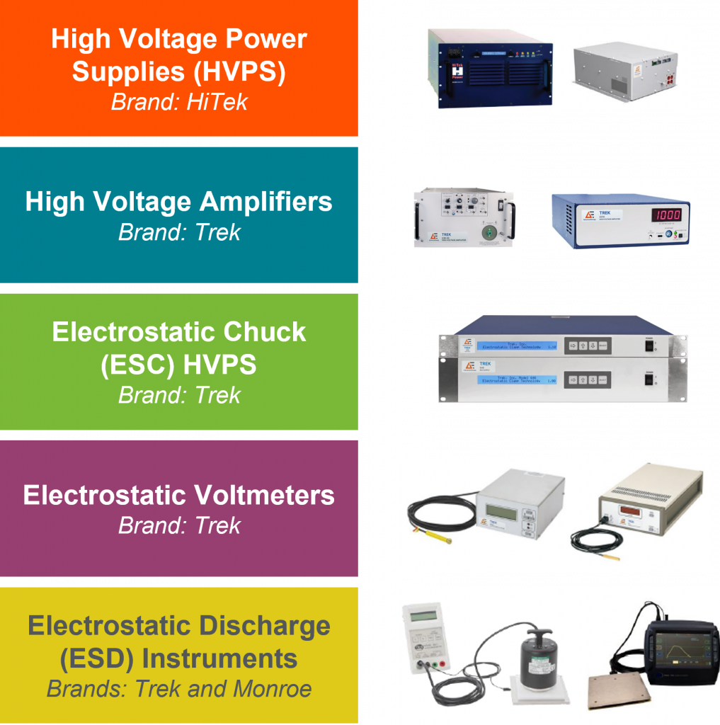
AE’s portfolio of standard, modular and custom high-voltage products for manufacturing technologies
However, the in-house expertise and experience available to semiconductor customers do more than just ensure that Advanced Energy can address existing demands – they also allow the company to anticipate future demands. This forward-looking approach empowers new, innovative solutions that will meet the coming needs of the industry based on a holistic view of market and technology trends. Examples of such application-specific development includes options for actionable, real-time intelligence to support process characterization and optimization and the bringing together of high voltage amplifier technology and arbitrary waveform generation to provide semiconductor tool manufacturers with a new way to control electrostatic chucks. This control ensures wafer detection, better clamping, more efficient de-clamp and minimum residual wafer charge.

Trek 645 Electrostatic Chuck High Voltage Power Supply
Expanding to Serve a Growing Market
Advanced Energy’s high-voltage business is dedicated to empowering new technologies and meeting the needs of transformative manufacturing technologies. As the market for high-voltage systems grows, so too does the investment that the company is making in its design, testing and production capabilities. This year alone will see further expansion of Advanced Energy’s Trek and Monroe products and, driven by rapidly growing demand for implant, etch, deposition, SEM and e-beam power, additional increases in capacity in Littlehampton, UK, which house the team dedicated to the HiTek product lines. These expansions underline Advanced Energy’s commitment our customers and ensure that the business is well-positioned to continue its work in identifying, designing and delivering critical high-voltage systems and supporting and optimizing customers’ fabrication processes.
Blog
The High-Voltage Innovations Behind Moore’s Law
Accurate Prediction of Vacuum Capacitor Lifetime Reduces Unplanned Downtime by 80%

The failure of any key element or subsystem in a semiconductor manufacturing facility has the potential to bring the process to a complete standstill and/or to force costly wafer scrap. A key consequence of such failure is an associated increase in the cost of operations. While rarely reflected in the upfront Capital Expenditures (CapEx) pricing, from a Total Cost of Ownership (TCO) perspective, manufacturers typically find that unplanned downtime, raw material wafer costs, unscheduled repairs and the purchase of spare units can be significant contributors to Operating Expenses (OpEx).
With today’s complex semiconductor manufacturing processes, operators are looking for ways to identify not only the potential points of failure but also ways to predict when a failure is most likely to occur. Armed with this information they can then proactively address problems before they lead to costly, productivity-impacting downtime.

Collecting and analyzing equipment data to create meaningful intelligence on which to base predictive maintenance has not always been easy. Now, with PowerInsight by Advanced Energy™, operators can obtain actionable insight from critical power delivery systems that will allow them to maximize performance and cut costs.
Take, for example, the need to predict the lifetime of the vacuum capacitors employed in many of today’s impedance matching networks. Thanks to AE’s proprietary algorithm and years of experience, customers can accurately predict when their vacuum capacitors need refurbishment, allowing them to reduce unplanned downtime by as much as 80 percent.
Determining the Remaining Life of Vacuum Capacitors
As a critical element in the plasma process, the impedance matching networks used for semiconductor manufacture must minimize process variability and deliver high levels of system uptime. One potential cause of failure in a matching network is the end of life of the vacuum capacitors that provide impedance variation. These components have a finite lifespan and will need to be replaced periodically during a network’s useful operating life.
It is difficult to determine how long a vacuum capacitor will last. According to Advanced Energy’s research, capacitors have a wide lifetime variation due to the almost unlimited number of unique tool setups and processes. The actual lifetime of a match network capacitor is dictated by usage pattern and application rather than being solely dependent on time or energy. Vacuum capacitor manufacturers provide an expected lifetime given in number of cycles across its capacitance range, which is traditionally very difficult to measure. Finding a way to predict this capacitor lifetime would deliver significant benefits by preventing unplanned downtime and costly maintenance of the wafer processing chamber and the match network. With AE’s PowerInsight, such prediction has become possible.
PowerInsight is a monitoring and analytics platform that has been specifically designed to bring actionable intelligence and insights to critical power delivery systems and allow operators to maximize performance, cut costs and improve yields. This platform can access more than 50 fields of internal processor and control data from Navigator® II, a rapid, accurate and reliable digitally-tuned matching network that delivers highly accurate RF plasma control.
In developing the solution, Advanced Energy’s in-house reliability lab conducted highly accelerated life testing to validate mechanical wear and failure models from the capacitor manufacturer. This testing provided the input to create the predictive models and analytics that would be used as the basis for determining capacitor life. Using data collected from Navigator II, PowerInsight uses proprietary algorithms to observe details of vacuum capacitor movements and compare them with historical usage patterns. This allows an estimation of the ‘consumed life’ of the capacitor. Using this estimation, coupled with the supposition that the observed usage patterns will be maintained, PowerInsight can project how much time and/or throughput remains until the unit should be scheduled for refurbishment.
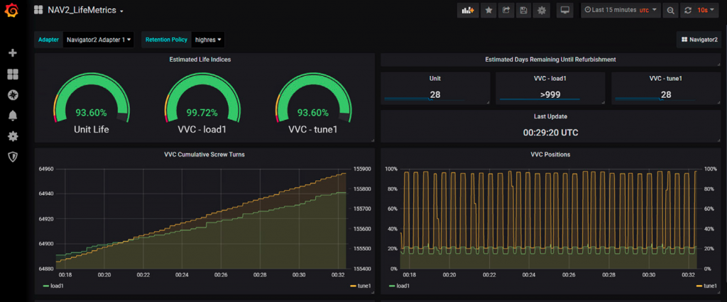
For many Advanced Energy products, including the Navigator II, PowerInsight uses a ‘plug-and-play’ hardware device with integrated edge computing capacity, known as the Explorer. In addition, the Ascent® SMS AP-10 is the first AE product with integrated PowerInsight capabilities. By connecting the Explorer to a browser, customers can immediately see data flow and customized analysis chart. An easy-to-use dashboard displays the percentage of life left for each vacuum capacitor, as well as an estimation of days left until a refurbishment will be required on the unit.
Customer Deployment
In the past, customers were faced with making refurbishments upon failure due to the inability to forecast vacuum capacitor lifetime. Now, thanks to AE’s proprietary algorithm and years of experience, they can take a highly proactive approach and accurately predict when their unit is at the recommended manufacturer refurbishment interval for the vacuum capacitors. This allows customers to maximize the useful life of their vacuum capacitors and reduce unplanned downtime by as much as 80 percent.

The Future of Semiconductor Manufacturing: Reflecting on the 2022 SEMI Industry Strategy Symposium

As a market leader in precision power conversion, measurement and control solutions for semiconductor manufacturing, Advanced Energy has long been a participant at SEMI’s Industry Strategy Symposium (ISS), the premier event to share the semiconductor industry’s outlook. Despite this year’s off-cycle event in April (compared to the typical mid-January), ISS saw record attendance.
The Importance of the Semiconductor Industry
A desire to better understand macro uncertainties and a strong Wafer Fab Equipment (WFE) market likely incentivized ISS attendance. A quick sweep of media headlines over the past two years highlights the growing significance of semiconductors to more and more industries. Entering 2022, there are increased uncertainties of the broader economy from supply chain constraints to inflation and rising interest rates and - more than ever - the entire semiconductor supply chain is playing a more important role as a “behind the scenes” driver of the economy. More government officials from both the federal and state level attended this year’s ISS, highlighting the growing importance of semiconductors to national security, the U.S. government’s focus on strengthening the semi supply chain, as well as new opportunities for governments to invest in supporting the semi equipment and materials companies.
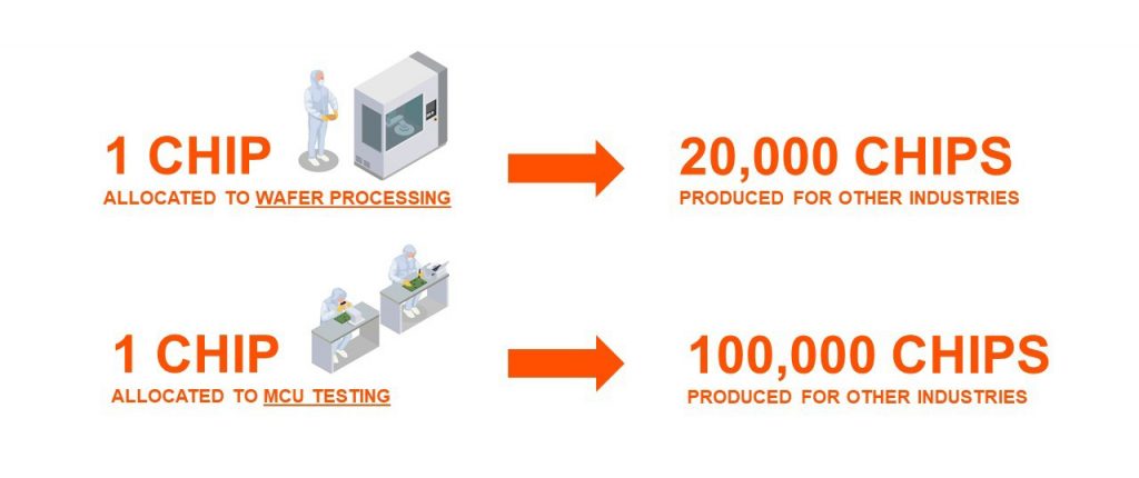
While the 2022 forecasts and the long-term outlook are equally optimistic, with some predicting that the semiconductor industry will reach $1 trillion in sales by 2030 followed closely by the semi equipment and materials industry, most agree that the supply chain remains the biggest risk. Several analysts believe that a downturn will likely occur before we reach this milestone given the cyclical nature of the industry but the timing of such a downturn is a subject of contention. The resolution of supply constraints will be critical to growth in 2022 and 2023. To improve supply constraints, chips must be allocated to the semi equipment industry to enable the creation of more chips. According to SEMI, each chip allocated to a wafer processing tool will produce at least 20,000 additional chips per year, and each FPGA allocated to a microcontroller (MCU) tester will test nearly 100,000 additional MCUs per year. One chip used in the semiconductor equipment industry produces many more chips for automotive, consumer electronics, data centers and other industries.
Semiconductor Process Technology Innovation
Resolving supply constraints is also critical to the pace of innovation beyond the semiconductor industry. At ISS, chipmakers highlighted the dependence of disruptive technologies such as Artificial Intelligence (AI) and Machine Learning (ML) on the semiconductor industry. The advancement in the leading-edge wafer processing and in advanced packaging processes have been critical to enable AI and ML applications. The exponential growth of AI computation usage is faster than Moore’s Law, powered by the substantial improvements in processor performance, as well as innovation in the wafer processing and equipment industry.
Three major technology trends are poised to drive advancements in leading-edge logic over the next several years:
1. Gate All Around at 2nm/1nm and CFET for <1nm
Gate-All-Around (GAA) is the most immediate technology inflection for the industry and allows the industry to continue to follow Moore’s Law. As advanced logic moves to 2nm node, GAA will be adopted by all three leading-edge companies. Since 2nm is already in development, GAA is currently the key battleground for leading equipment OEMs. The architectural change from FinFET to GAA will require many new process steps, which will ultimately drive increased demand for advanced etch, deposition, epi and PEALD process equipment. At ISS, Tokyo Electron detailed the process complexity of creating a GAA device and ASM discussed its new PEALD processes to create nanotube gates. In addition, LAM Research recently launched new etch products designed for GAA.
At Advanced Energy, we have been working closely with our OEM customers to develop next-generation process power solutions that will enable many of those new processing steps necessary to create future generation of devices, from Nanosheet GAA and Forksheet GAA to CFET and beyond.
2. Backside power
Chipmakers are targeting to change the back-end-of-line (BEOL) interconnect to substantially drive improved power efficiency and transistor density, critical to enable continued scaling down to sub-2nm and beyond nodes. Historically, BEOL is created after the transistors are formed on the wafer but new backside power architecture intends to move a number of metal layers to the “back” by sandwiching the transistors between front and back side metal layers. This is done by creating two individual wafers and attaching them together. The shift to backside power will require new etch and deposition processes to create the interlayers, with new process steps and films likely to be required. To enable this change, new processing power solutions and potentially new breakthrough power deliver solutions will be needed. Advanced Energy has been the market leader in process power solutions and will continue its leadership in enabling many next-generation etch, depositions, implant, inspection and other processing tools.
3. Chiplet or die stacking in 3D packaging
2.5D and 3D packaging have already been widely used across many semiconductor devices but this is just the beginning. Known as chiplets, dies or tiles of different function are integrated together using advanced packaging techniques to create more powerful chips that are also more cost efficient. Much has been written about the variety of 2.5D/3D package structures but at this year’s ISS, there is growing evidence of the increased innovations that are being developed to create these complex packages. From AMD’s transition to a 3D chiplet that comes with over 200X increase in interconnect density to Intel’s next-gen Foveros Direct technology with 40x interconnect bump density, there is less separation between wafer processing and packaging in chiplet architecture. Historically, the industry mostly used tools built for wafer processing or legacy packaging equipment to create the 2.5D packaging architectures. However, new technologies and equipment are being developed specifically to create 3D packages. Naturally, the new equipment will come with new and likely more complex power requirements and Advanced Energy is ready to meet these challenges.
Over the past 40 years, Advanced Energy has been at the forefront of developing next-generation power solutions to drive advanced nodes. AE continues to innovate the future of power in semiconductor manufacturing processes. The heart of critical etch and deposition processes will continue to be plasma-driven, led by a new generation of plasma power solutions such as Advanced Energy’s eVoS™, our asymmetric bias waveform generator, and Navigator II FCi, our high speed solid state match.
Workforce Development and Diversity & Inclusion
It’s an exciting time for the industry, with advances in semi manufacturing processes translating into innovations in intelligent, revolutionary technologies that touch and improve all aspects of life. But for the semiconductor industry to move forward, workforce development and diversity and inclusion must be at the forefront. It was encouraging to hear the efforts the semiconductor industry has put into nurturing a diverse, workforce-ready talents at ISS with presentations from industry thought leaders, leading companies, universities and students. It was also exciting to hear presentations from a diverse group of students and get a glimpse of the next-generation of industry leaders. One solution to address the under-representation of minority groups is to expand the talent pipeline and allow students from these groups to explore opportunities in STEM. For example, Advanced Energy’s STEM Diversity Scholarship Program aims to develop emerging talent and promote greater diversity in STEM. Not only does this help fill the industry pipeline with qualified talent, the program also cultivates new and different perspectives that help drive technological innovations that positively impact society.

Blog
The Future of Semiconductor Manufacturing: Reflecting on the 2022 SEMI Industry Strategy Symposium
Optimized Power, Not More Power: Plasma Power for Next-Generation Semiconductor Wafer Fabrication

As integrated circuit (IC) designs become ever-more complex with each new architecture and technology node, so does the processing of the semiconductor wafers used to fabricate those ICs. Among the challenges faced by semiconductor manufacturing equipment OEMs and wafer manufacturers, for example, is how to meet demands for narrower line widths and straighter, deeper features for advanced deposition and etching techniques. In addition, the same OEMs and wafer fabs are under pressure to keep electric power usage as low as possible while maximizing throughput – the importance of rapid, high yield product is made abundantly clear by the global impact of this year’s semiconductor shortage.
One of the most critical process steps is High Aspect Ratio (HAR) etch. With HAR features being fabricated at >100:1 aspect ratios, etching to the bottom of these features has driven the power requirement of an etcher towards an unsustainable level of over one MW per tool.
As some thought leaders in IC manufacturing have pointed out, the industry has been trying to solve an exponential problem with a linear solution. One way to address the challenge is to re-think how power is delivered and managed in plasma-based applications such as etch and deposition. In particular, the growing need for more precise process control and more targeted and efficient power delivery – as well as improved yields by reducing the potential for heat damage – is driving semiconductor manufacturers to look beyond traditional sinusoidal RF bias power techniques and consider alternative approaches that enable new process characteristics.
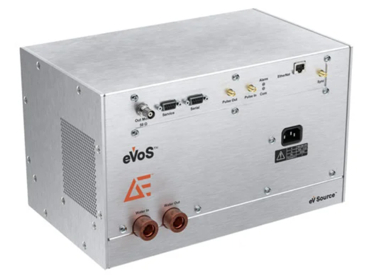
It is with this in mind that Advanced Energy developed the next leap beyond conventional high-power RF. Leveraging four decades of leadership in highly engineered power solutions, the company has developed the eVoSTM asymmetric bias waveform generator for leading mode, critical plasma applications.
eVoS is an integrated, solid-state high-voltage system that delivers the first direct ion energy “knob.” It applies metrology and proprietary waveform control to deliver precise plasma bias performance needed for sensitive feature formation in high-aspect-ratio structures at high etch rates. eVoS features customizable and direct Ion Energy Distribution Function (IEDF) control, as well as real-time output monitoring.
Offering direct control of ion energy distribution in plasma processing applications, the eVoS power source integrates a bi-directional voltage supply and independent current source to establish and control wafer-surface potential. The asymmetric waveform greatly reduces power transfer inefficiencies inherent to the use of sinusoidal RF power in bias applications while providing more precise ion energy control and supporting faster etch rates.
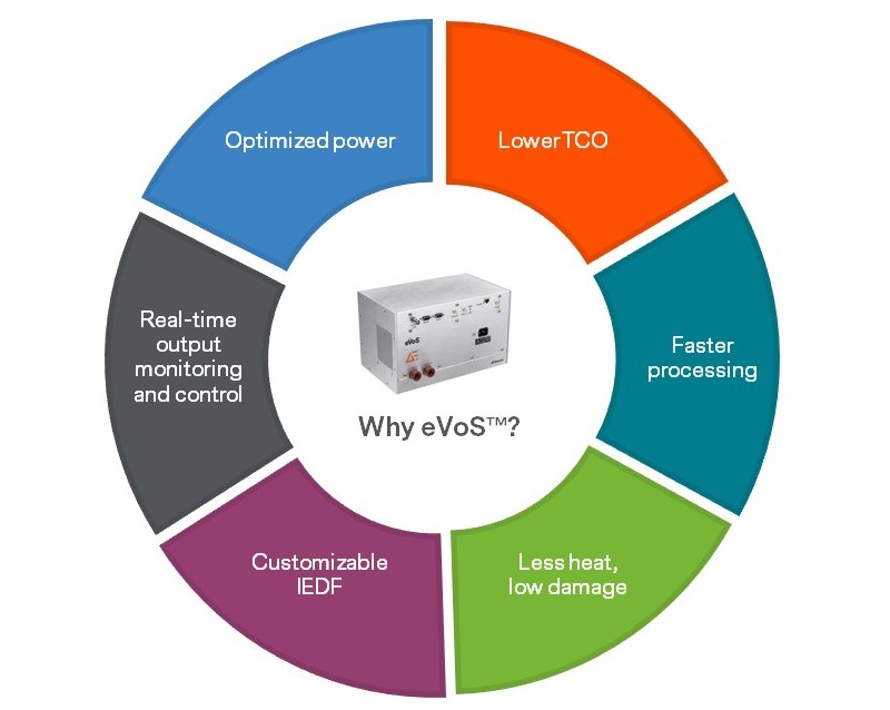
Unlike conventional sinusoidal RF power sources, the eVoS platform’s fast digital metrology and novel control algorithms enable the production of near mono-energetic ion energy distributions (IEDs) that deliver power only where the plasma needs it. This, in turn, ensures maximum efficiency and optimized energy use. eVoS breaks a trend that has been pushing power requirements up to 100 kW per plasma chamber and as much as 1 MW per etcher by supporting advanced fabrication processes with as little as half or even a third of those power demands for superior etch profiles and higher etch rates. In addition, because precise control produces less unused power, the potential for wafer damage due to heat is also reduced. This translates to lower overall total cost of ownership (TCO) compared to RF delivery systems.
As Abraham Maslow eloquently stated, it is tempting to treat every problem like a nail if the only tool available is a hammer. eVoS provides OEMs with another tool in their toolbox – a novel solution for optimized application of bias power beyond RF that enables new methods for process tuning and control.

Blog
Optimized Power, Not More Power: Plasma Power for Next-Generation Semiconductor Wafer Fabrication
Making the Switch at Speed
With the goal of enabling faster semiconductor manufacturing plasma processes, Advanced Energy (AE) threw the switch on a radical development program back in 2010 to develop and launch the industry’s fastest RF power tuning network. In 2020, we launched our latest, even faster, solid-state tuning network with sub-millisecond response times with the introduction of the Navigator® II FCi. With these milestones, we not only transformed the industry by developing the fastest RF tuning networks, but we also changed ourselves by learning to deliver product innovations radically faster.
The semiconductor industry’s relentless pursuit to pack ever-increasing performance in smaller packages drives thinner films and narrower linewidths. In many applications, this means very short process steps with plasma transition times faster than conventional vacuum capacitor-based tuning networks can react.
We pioneered solid-state RF matching (tuning) technology for semiconductor plasma processes in the 1990s. Over the past 20 years, we’ve shipped more than 20,000 RF delivery systems with integrated solid-state matching networks built into those systems. These innovations met the critical industry need for ultra-fast tuning with millisecond response timeframes.
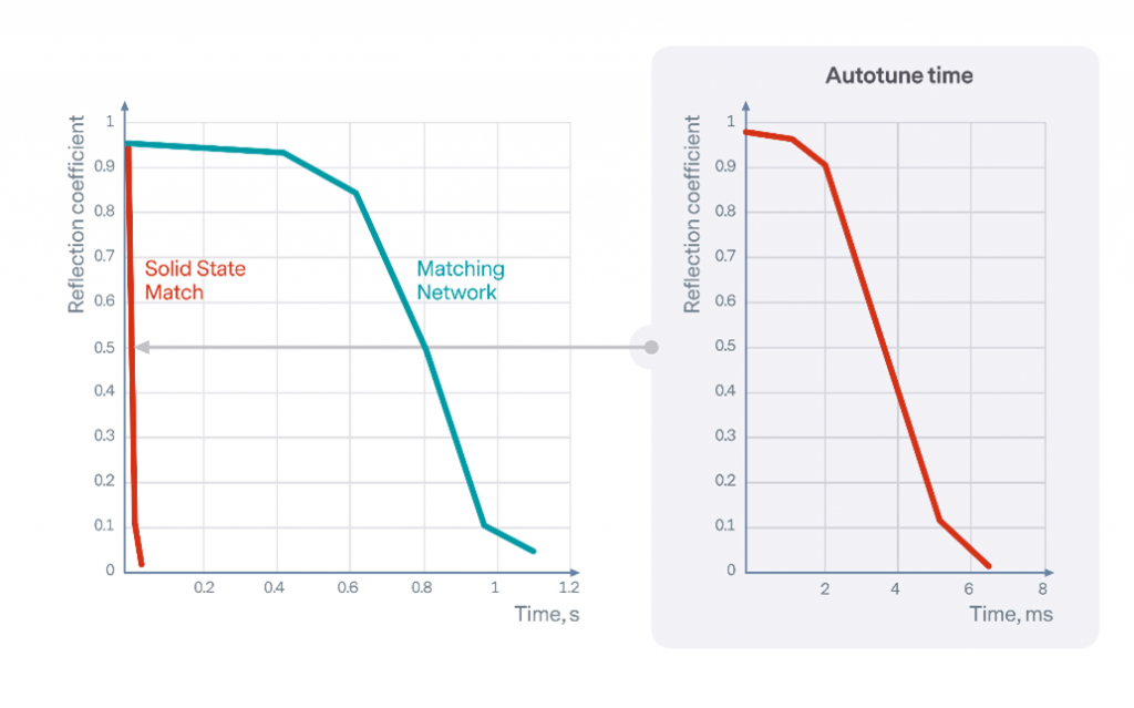
Typical tuning time of a traditional matching network (blue line) and a solid-state match (red line) on a plasma chamber are compared in the left graph. The expanded view of the SSM tuning trace on the right shows that full tuning can be achieved in the millisecond timescale, compared with hundreds of milliseconds for a traditional match.
Around 2010, there was a rapid expansion in the number of new applications that could leverage ultra-fast, millisecond tuning, such as Atomic Layer Deposition (ALD). There was also a growing need for the flexibility to have independent, stand-alone, solid-state matching networks —rather than fully integrated into an RF delivery system. A stand-alone solid-state match would enable an additional range of innovations where the RF generator(s) could be more specifically optimized for the overall, often multi-frequency, RF circuit.
To meet the growing customer needs, AE set out to quickly deliver a stand-alone solid-state matching product. At that time, Yuval Wasserman, who was AE’s COO at that time and is currently AE’s CEO, made a bold decision: “AE would develop a fully novel stand-alone solid-state matching network platform in less than a year.” Typically, new technology development from the ground up would take two or more years, which made this a very loft goal. Upending traditional product development approaches, Yuval pulled together a kind of “AE-Skunk Works” that coincidentally leveraged Lockheed’s Skunk Work approach and Kelly Johnson’s 14 Rules and Practices, such as:
- #2: Viciously minimize the team
- #3: Collocate somewhere small
- #4: Isolate the team with strictly controlled security measures
- #7: Involve the whole team in the big picture
- #8: Reward performance, not status
AE’s bold shift came following the severe 2009 industry downturn where any investments were under incredible scrutiny and the industry generally hove to more incremental approaches. Undeterred, the AE’s solid-state match “skunk works” team kicked off in 2010, and quickly developed the technology and secured initial patent priority dates throughout 2011 before introducing the product to partner customers in closed-door events at SEMICON West 2011.
This switch proved a success. Following customer early learning shipments, the solid-state Navigator II FastCap™ was launched to the broader market one year later at SEMICON West 2012 and set the bar as the fastest stand-alone RF plasma power matching network.
Building on the success of the Navigator II FastCap, we introduced Navigator II FCi in 2020. This new, faster solid-state matching network again raised the bar on RF matching network speeds to sub-millisecond processes. With broadened power and impedance ranges and an ultra-fast turning speed, Navigator FCi enables next-generation applications such as Atomic Layer Etch (ALE).
The Navigator II FastCap program was a monumental switch in AE’s program development process and brought solid-state matching to meet a critical market need. As we look to the future, keep watching AE as we continue to “switch it up” to meet our customers’ fast-evolving needs.
.png?resizemode=force&maxsidesize=884)
20 Years of No Strings Attached Performance
“No strings attached performance” in RF plasma power for semiconductor manufacturing? Here at Advanced Energy (AE), we like to say, “no cables attached performance.” This was just one of the five daunting challenges we solved when designing our unique genre-breaking RF plasma power delivery system:
- No cables from RF generator-to-match and match-to-process chamber electrode
- Ultra-fast RF tuning for very short process steps
- Wide impedance operating range
- A compact single package to fit in small spaces (enabling direct connection to chamber)
- Less expensive than traditional RF generator + matching network + connectors + cables
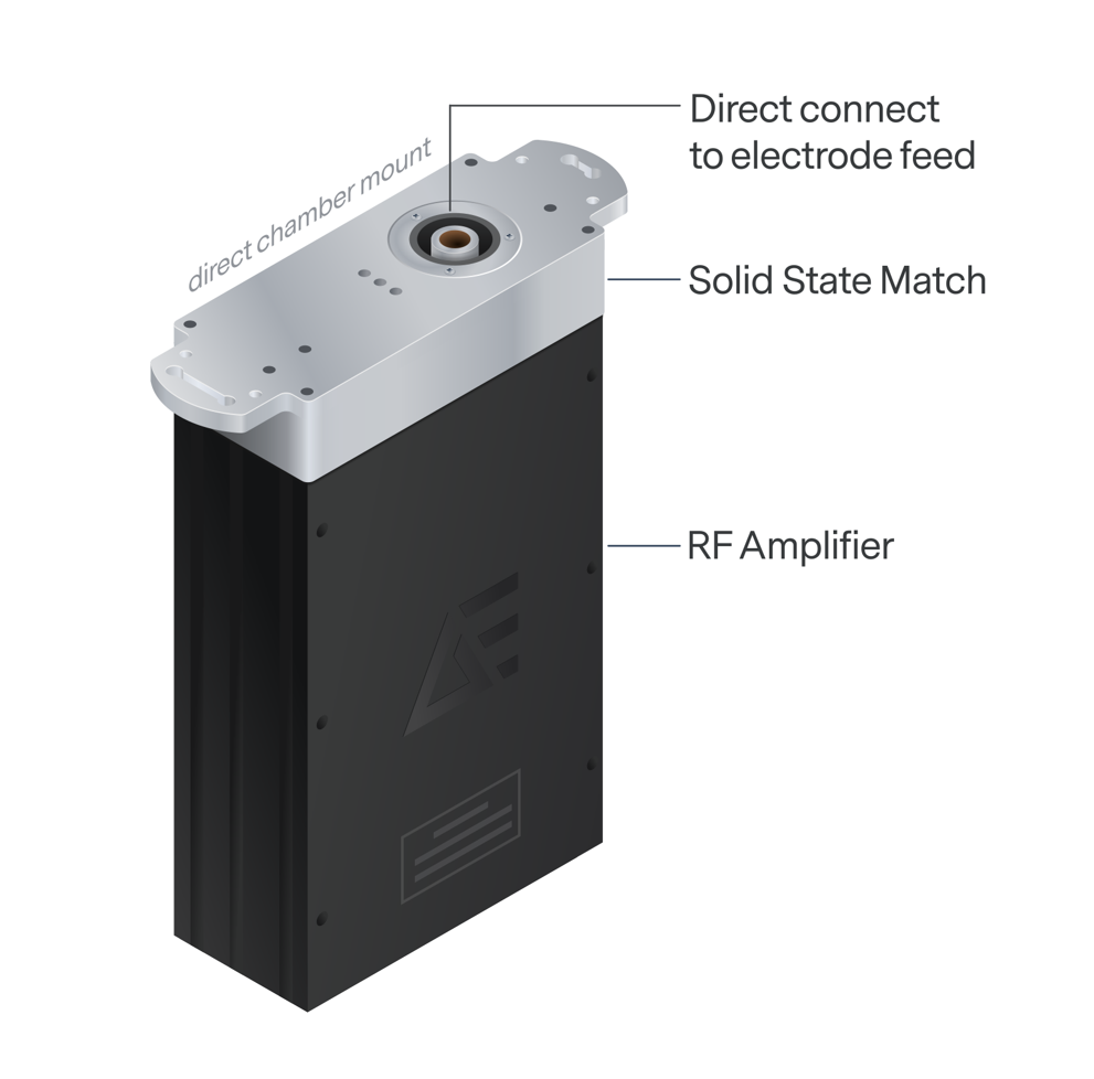
Twenty years ago, we pioneered the first commercially viable, fully integrated RF generator and solid-state matching network system … and it’s been a massive success. Since then, we’ve shipped more than 20,000 RF delivery systems with “no cables attached performance” to customers around the world. What began in the year 2000 with our first production volume shipments of the fully integrated system has now evolved into the Paramount® HFi™ – today’s all-digital, integrated generator and solid-state match system.
To meet the demand for a small footprint in advanced semiconductor processing tools such as PECVD and plasma Etch, we developed the most compact and highest performing integrated RF delivery system available. With a package size of 8.5” (W) x 16.5” (D) x 5.25” (H), the HFi products have been recognized for segment-best power density record (~0.25 watts/cm3). The compact package, which would be substantially smaller than a combination of a standard RF generator and a match network, makes it ideal for integrating right onto the process chamber, where space is often limited.

In the Paramount HFi, an electrically switchable solid-state capacitor array is physically integrated with the RF power amplifier providing the most compact form-factor power delivery system available.
It turns out good things do come in small packages – especially when it comes to controlling plasma processes. Paramount HFi delivers the fastest response times with sub-millisecond regulation for crisp transitions on even the shortest process steps at over 32 tune range positions. As seen in the first graph below, typical power delivery of an RF match based on the variable vacuum capacitor could take 0.75 seconds of fluctuation before reaching a new setpoint. Comparing this slow response to the second graph, AE’s solid-state match response with direct coupling to the process chamber makes process transitions into nearly vertical step functions. With nimble, wide-range solid state matching, the HFi series has become an enabler for future generations
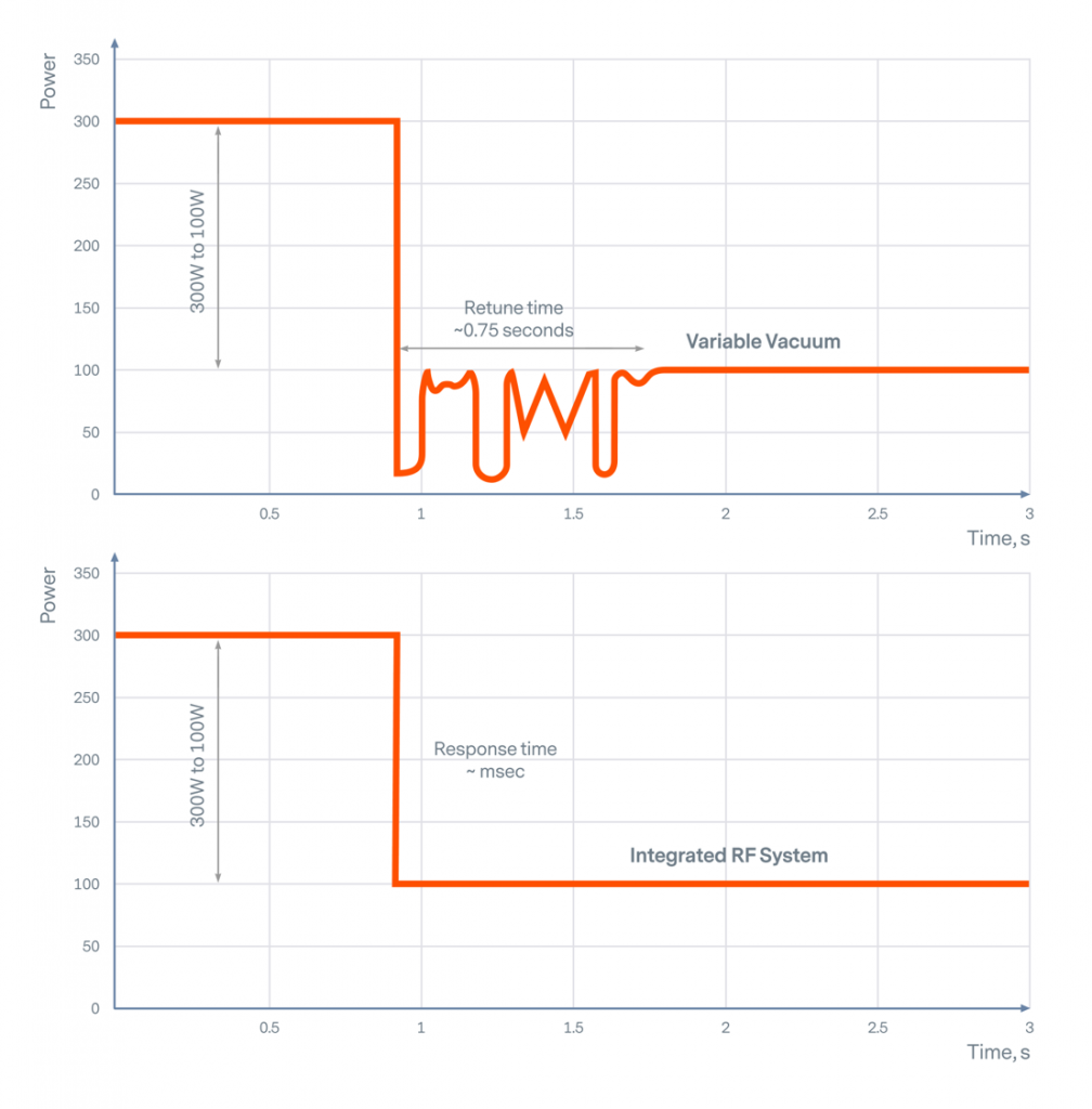
The Paramount HFi delivers power to a setpoint change from 300 to 100 W within a millisecond timeframe. This ensures constant, repeatable power delivery where the near-instant tuning increases productivity for these very short, high-cycle count plasma deposition processes.
After 20 years and 20,000 units shipped, our “no strings attached performance” is just hitting its stride alongside our latest innovations.
.png?resizemode=force&maxsidesize=884)
Precise Power Control and Unmatched Reliability with the New MAXstream RPS
I’m pleased to update you on the release of Advanced Energy’s new line of MAXstreamTM remote plasma source (RPS) systems. MAXstream RPS is a huge leap forward, and leverages AE’s plasma power and RPS product experience, providing customers with more precise power control and improved design flexibility while maintaining industry-leading reliability.
RPS chamber cleaning is an essential part of the chemical vapor deposition (CVD) process in semiconductor manufacturing. During CVD film deposition on the wafer, film residue deposits build up on the inside walls of the process chamber and can impact the wafer deposition process itself. RPS systems allow customers to perform periodic inline cleaning of the CVD chamber to maintain process stability and cleanliness. The RPS system uses a Radio Frequency (RF) generated plasma to dissociate gases, such as NF3, to clean the chamber. The fluorine radicals generated by the RPS system flow into the CVD chamber, reacting with residue on the chamber walls to form a gaseous product, which is then pumped away in the exhaust to the abatement system. This process effectively cleans the chamber walls and ensures the on-wafer CVD deposition does not drift due to changing chamber conditions.
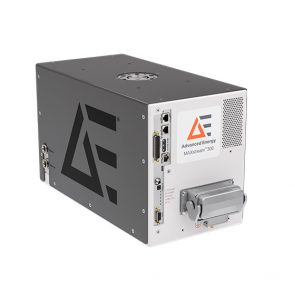
Advanced Energy's MAXstream 300 Remote Plasma Source
Customer feedback by both OEM CVD manufacturers and the end-users of CVD tools drove the development of AE’s MAXstream. Customers identified RPS reliability and lifetime as critically important factors to them; after all, fabs only make money when their process tools are running. To this end, AE designed MAXstream RPS to be the longest life, most reliable RPS system available on the market. The MAXstream chamber uses a proprietary aluminum formulation with type III hard coat anodization, providing a longer chamber lifetime than alternative designs. MAXstream also uses a sophisticated chamber wall cooling system that minimizes thermal gradients which can cause chamber coating degradation. When MAXstream does need service, customers have access to Advanced Energy’s best-in-class global service and support network, with over a dozen local service centers for fast, experienced assistance.
Beyond reliability, MAXstream offers a leap forward in cleaning performance. All MAXstream flow and power ranges provide industry-leading 2% power accuracy and a unique dual-ignition system that ensures consistent plasma ignition. Customers have also told us that it is important to have an easy way to incorporate MAXstream into their new and existing process tools, so AE designed MAXstream to have dimensional and utility hookup compatibility with existing RPS products in the market. This form factor provides OEMs and end-users an easy, drop-in way to upgrade their RPS to MAXstream’s reliability and improved performance, without requiring redesign or replumbing of the CVD tool.
The complete product line consists of the MAXstream 300, 600, 800, 1000, and 1200 systems. The MAXstream 600 to 1200 serve the higher-flow RPS market, with NF3 flow rates of 6 to 12 slpm. The MAXstream 300 is a smaller form factor tool that can provide up to 3 slpm of NF3 flow for customers who need a more compact, lower cost-of-ownership solution for low flow applications. AE is now shipping MAXstream evaluation systems to our OEM customers, with general availability scheduled in the first quarter of 2021.
.jpg?resizemode=force&maxsidesize=884)