Optimized Power, Not More Power: Plasma Power for Next-Generation Semiconductor Wafer Fabrication
已发布 十二月 02, 2021 由 Dhaval Dhayatkar

As integrated circuit (IC) designs become ever-more complex with each new architecture and technology node, so does the processing of the semiconductor wafers used to fabricate those ICs. Among the challenges faced by semiconductor manufacturing equipment OEMs and wafer manufacturers, for example, is how to meet demands for narrower line widths and straighter, deeper features for advanced deposition and etching techniques. In addition, the same OEMs and wafer fabs are under pressure to keep electric power usage as low as possible while maximizing throughput – the importance of rapid, high yield product is made abundantly clear by the global impact of this year’s semiconductor shortage.
One of the most critical process steps is High Aspect Ratio (HAR) etch. With HAR features being fabricated at >100:1 aspect ratios, etching to the bottom of these features has driven the power requirement of an etcher towards an unsustainable level of over one MW per tool.
As some thought leaders in IC manufacturing have pointed out, the industry has been trying to solve an exponential problem with a linear solution. One way to address the challenge is to re-think how power is delivered and managed in plasma-based applications such as etch and deposition. In particular, the growing need for more precise process control and more targeted and efficient power delivery – as well as improved yields by reducing the potential for heat damage – is driving semiconductor manufacturers to look beyond traditional sinusoidal RF bias power techniques and consider alternative approaches that enable new process characteristics.
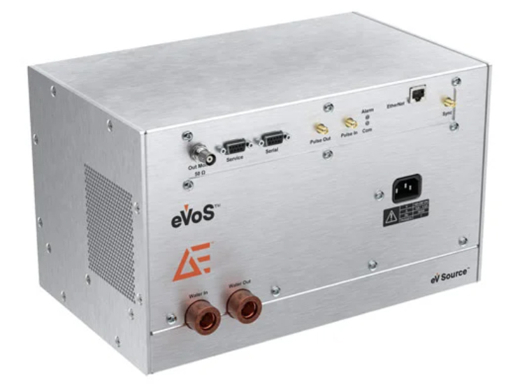
It is with this in mind that Advanced Energy developed the next leap beyond conventional high-power RF. Leveraging four decades of leadership in highly engineered power solutions, the company has developed the eVoSTM asymmetric bias waveform generator for leading mode, critical plasma applications.
eVoS is an integrated, solid-state high-voltage system that delivers the first direct ion energy “knob.” It applies metrology and proprietary waveform control to deliver precise plasma bias performance needed for sensitive feature formation in high-aspect-ratio structures at high etch rates. eVoS features customizable and direct Ion Energy Distribution Function (IEDF) control, as well as real-time output monitoring.
Offering direct control of ion energy distribution in plasma processing applications, the eVoS power source integrates a bi-directional voltage supply and independent current source to establish and control wafer-surface potential. The asymmetric waveform greatly reduces power transfer inefficiencies inherent to the use of sinusoidal RF power in bias applications while providing more precise ion energy control and supporting faster etch rates.
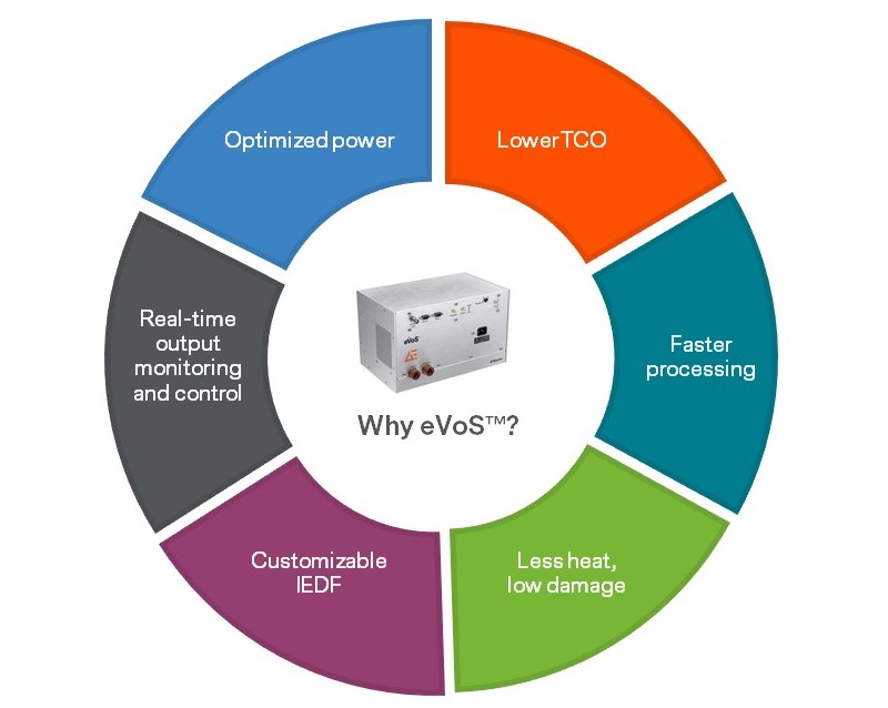
Unlike conventional sinusoidal RF power sources, the eVoS platform’s fast digital metrology and novel control algorithms enable the production of near mono-energetic ion energy distributions (IEDs) that deliver power only where the plasma needs it. This, in turn, ensures maximum efficiency and optimized energy use. eVoS breaks a trend that has been pushing power requirements up to 100 kW per plasma chamber and as much as 1 MW per etcher by supporting advanced fabrication processes with as little as half or even a third of those power demands for superior etch profiles and higher etch rates. In addition, because precise control produces less unused power, the potential for wafer damage due to heat is also reduced. This translates to lower overall total cost of ownership (TCO) compared to RF delivery systems.
As Abraham Maslow eloquently stated, it is tempting to treat every problem like a nail if the only tool available is a hammer. eVoS provides OEMs with another tool in their toolbox – a novel solution for optimized application of bias power beyond RF that enables new methods for process tuning and control.

Dhaval Dhayatkar
相关帖子

Blog
.jpg?resizemode=force&maxsidesize=884)